


|
Live Session 1*
Tuesday
December 3rd 2024 |
Live Session 2*
Tuesday
December 3rd 2024 |
| 10 am CET / Berlin 5 pm SGT / Singapore 6 pm JST / Tokyo |
5 pm CET / Berlin 8 am SGT / Los Angeles 11 am JST / New York |
* the content of both sessions is identical
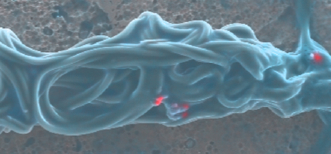
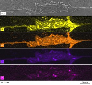
What to expect? Analytical electron microscopy (EM) techniques such as energy-dispersive X-ray spectroscopy (EDS) are invaluable for studying biological samples containing minerals like calcium carbonate (CaCO₃), metal ions, or other compositions beyond carbon and oxygen. However, analyzing beam-sensitive materials can be challenging due to their low signal output and long acquisition times, often leading to sample damage and loss of the measured area. The XFlash® FlatQUAD detector was utilized to overcome these challenges, enabling the study of beam-sensitive organic materials, particularly frozen biological samples in scanning electron microscopy (SEM). In this webinar, our guest speaker, Dr. Ifat Kaplan will present the cryo-SEM-EDS workflow, along with imaging and spectral data that reveal the distribution of metal ions during silk processing in silkworms. SEM EDS mapping under cryo-conditions reveals the composition and spatial localization of metal ions during silk evolution within the silk gland. These findings were recently published in *Nature Communications* (*O. Brookstein et al., 2024, DOI: 10.1038/s41467-024-50879-9*). Join us for this informative 30-minute session to learn about the exceptional performance of the XFlash® FlatQUAD, a highly sensitive EDS detector for SEM, which is optimial for chemical mapping of biological and life science specimens. Discover how this cutting-edge technology handles even the most challenging samples with unparalleled speed (10x–50x faster compared with conventional EDS detectors) and sensitivity, making it a top choice for SEM EDS analysts.
![]() What makes the XFlash® FlatQUAD an ideal detector for chemical mapping of life science specimens.
What makes the XFlash® FlatQUAD an ideal detector for chemical mapping of life science specimens.
![]() Limitations of conventional large-area EDS detectors for analyzing biological materials.
Limitations of conventional large-area EDS detectors for analyzing biological materials.
![]() Benefits of low-kV chemical mapping with EDS in SEM.
Benefits of low-kV chemical mapping with EDS in SEM.
![]() Fast chemical mapping of light elements (Up to Boron) in biological samples using SEM EDS.
Fast chemical mapping of light elements (Up to Boron) in biological samples using SEM EDS.
Who should attend?
![]() Researchers, students, and industry professionals focusing on chemical analysis of biological materials.
Researchers, students, and industry professionals focusing on chemical analysis of biological materials.
![]() SEM and TEM users seeking advanced techniques for characterizing life science specimens.
SEM and TEM users seeking advanced techniques for characterizing life science specimens.

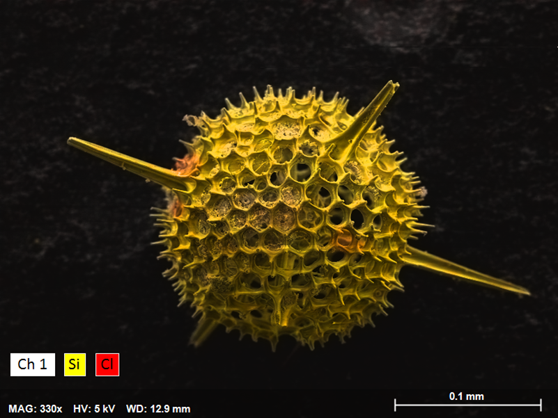
Chemical distribution map of a heavily charging pharmaceutical sample (multivitamin tablet) at 10 kV and low probe current (< 150 pA) with a short measurement time (67 seconds) and high count rate of 46,700 cps.
Ultra-high resolution SEM EDS map of a bulk FinFET structure acquired at 5 kV with XFlash® FlatQUAD with a high countrate of 309,000 cps in 90 seconds. The peak overlaps of Si-K (1.74 keV), W-M (1.81 keV) and Hf-M (1.67 keV) X-ray lines are automatically deconvoluted during acquisition.
Our Speakers
 |
Dr. Ifat Kaplan-AshiriAssociate Staff Scientist |
 |
 |
Dr. Purvesh SoniApplication Scientist EDS |
 |
Can't Attend the Live Webinar?
Don't worry if you can't attend the live webinar - Register anyway and we will send you the webinar recording and slides shortly after the webinar broadcast.
Can't Attend the Live Webinar?